
SiC trench MOSFET with dual shield gate and optimized JFET layer for improved dynamic performance and safe operating area capability
2023-12-02 09:23:06JinPingZhang張金平WeiChen陳偉ZiXunChen陳子珣andBoZhang張波
Chinese Physics B 2023年11期
Jin-Ping Zhang(張金平), Wei Chen(陳偉), Zi-Xun Chen(陳子珣), and Bo Zhang(張波)
1State Key Laboratory of Electronic Thin Films and Integrated Devices,University of Electronic Science and Technology of China,Chengdu 610054,China
2Chongqing Institute of Microelectronics Industry Technology,University of Electronic Science and Technology of China,Chongqing 401331,China
Keywords: SiC trench MOSFET,switching power loss,figure of merit,safe operating area
1.Introduction
Silicon carbide metal–oxide–semiconductor field-effect transistor (SiC MOSFET) is suitable for high frequency and high voltage applications owing to its material properties.[1,2]It opens the ways to diverse industries, including new energy vehicles,rail transit,and smart grids.In these applications,it is necessary to deal with short circuit, high temperature, and other extreme cases, which requires SiC MOSFET to be improved not only in performance, but also in reliability.SiC planar gate MOSFET demonstrates good reliability and has been commercialized for a long time.Compared with the planar counterparts,SiC trench gate MOSFETs(TMOSs)are preferred to further improve the device performance, owing to higher channel density and absence of junction field-effect transistor (JFET) region.[3]However, in the case of conventional TMOS,the high electric field present in the trench oxide during the blocking state leads to premature breakdown prior to the drain bias reaching an avalanche breakdown voltage(BVav).
With the development of the material and device manufacturing technology, many methods to optimize the SiC MOSFET structure have been proposed.Rohmet al.proposed an SiC double trench MOSFET(DTMOS)with a heavily doped p-type shielding region (P+SLD) at the sidewall and bottom of the source trench.[4,5]The DTMOS achieves an ultra-low specific on-resistance(Ron,sp).However,its large gate capacitance causes high switching power loss (Psw).In comparison with the DTMOS, the asymmetric TMOS (ATMOS) proposed in Refs.[6,7] shows better robustness, owing to the shielding effect provided by the half-surrounded P+SLD.[8]However, the inherently large MOS channel density of the trench structures results in a large saturation drain current(Id,sat),which reduces the short-circuit(SC)withstand time(tsc)and limits the improvement of the short circuit safe operating area (SCSOA).To further improve the switching characteristics and reduce thePsw,split/shield gate(SG)is introduced in Refs.[9–11].Introducing SG is an effective way to reduce gate–drain capacitance (Cgd).Moreover, unlike the Si counterpart, a thicker shield gate oxide thickness(Tsgox)is conducive to alleviating the maximum electric field in the gate oxide (Eox,peak) for the SiC SG-TMOS, which improves the gate oxide reliability.However,the coupling between the gate and source electrode still brings about large gate–source capacitance (Cgs) and the switching speed improvement is limited.
In this paper, a novel SiC trench MOSFET with a dual shield gate(DSG)and optimized JFET layer(ODSG-TMOS)is proposed.Compared with the conventional ATMOS(Con-ATMOS),the proposed structure shows good trade-off among theRon,sp,breakdown voltage(BV),and gate oxide reliability.The DSG structure reduces not onlyCgdbut alsoCgssignificantly.Therefore,the gate–drain charge(Qgd)and gate charge(Qg)are both reduced.As a result,the switching speed is improved and thePswis reduced, which significantly improves the dynamic performance.In addition,thetscis increased withId,satdecreasing and the large-current turn-off capability is also enhanced substantially.
2.Device structure and mechanism
Figures 1(a) and 1(b) show schematic cross-sectional view of the proposed ODSG-TMOS and Con-ATMOS, respectively.Both devices have an asymmetric trench gate structure on the surface.Compared with the Con-ATMOS,the proposed device features a fin-shaped gate which is surrounded by dual source-connected SGs and an L-shaped JFET layer.The shielding effect provided by the lower SG conduces to reducing theCgdand the reduced overlapping area between the narrower fin-shaped gate and lower SG creates reducedCgs.Apart from that,the interaction between the gate and the side wall of the source-connected P+SLD for the Con-ATMOS is transformed into the interaction between the fin-shaped gate and fin-shaped source-connected SG.Since the oxide layer between the two fin-shaped electrodes is much thicker than that at the side wall of the gate trench,the interaction between them is greatly decoupled,which can further reduce theCgsof the proposed structure.Therefore,the reverse transfer capacitance(Crss),input capacitance(Ciss),gate charge(Qg)as well as gate–drain charge(Qgd)are reduced,which improve the dynamic performance of the device.Furthermore, the thicker oxide layer of the DSG reduces the peak electric field at the trench corner, and combined with an optimized JFET layer,Ron,spis reduced without sacrificing theBV.In addition,since the lower SG is connected to the source,its potential remains 0 V instead of the gate drive voltage of 15 V or 18 V when the ODSG-TMOS is under saturation.Therefore,electrons do not gather near the side wall nor in corner of the lower SG.The depletion region is expanded widely in that region,which reduces the width of electron conduction path and enhances the JFET effect.As a result, theId,satis reduced and thetscis increased.By using the Silvaco TCAD with the modified models used in our previous work, such as band gap narrowing (BGN), CONSRH, CONWELL, SULFMOB, incomplete ionization,Auger and analytic models,the performance of the device is simulated.[11–13]The device parameters used in the simulation are shown in Table 1.The parameters not listed are the same for the two structures.The device areas used in this work for the two devices are both 1 cm2,unless otherwise mentioned.
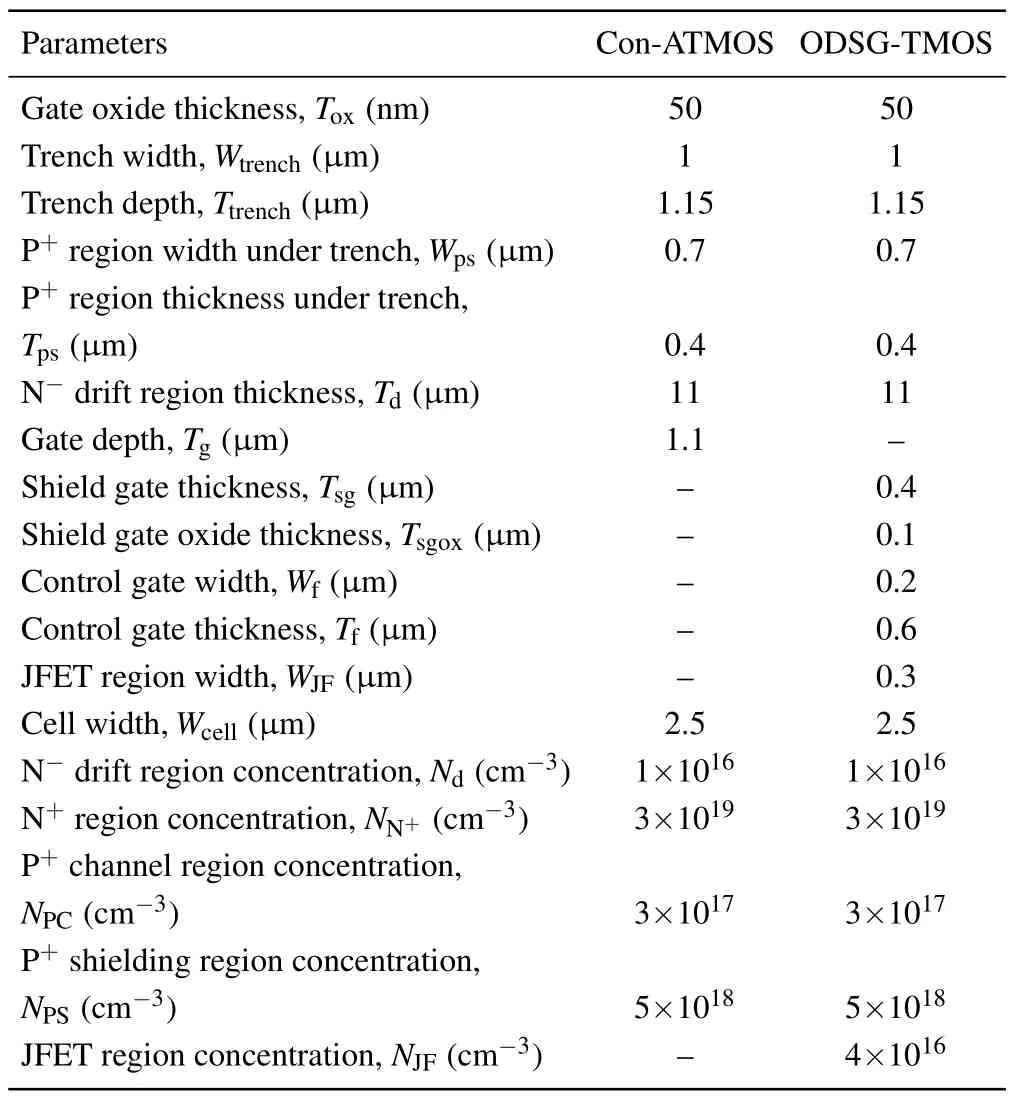
Parameters Con-ATMOS ODSG-TMOS Gate oxide thickness,Tox (nm) 50 50 Trench width,Wtrench (μm) 1 1 Trench depth,Ttrench (μm) 1.15 1.15 P+ region width under trench,Wps (μm) 0.7 0.7 P+ region thickness under trench,Tps (μm) 0.4 0.4 N- drift region thickness,Td (μm) 11 11 Gate depth,Tg (μm) 1.1 –Shield gate thickness,Tsg (μm) – 0.4 Shield gate oxide thickness,Tsgox (μm) – 0.1 Control gate width,Wf (μm) – 0.2 Control gate thickness,Tf (μm) – 0.6 JFET region width,WJF (μm) – 0.3 Cell width,Wcell (μm) 2.5 2.5 N- drift region concentration,Nd (cm-3) 1×10¹⁶ 1×10¹⁶ N+ region concentration,NN+ (cm-3) 3×10¹⁹ 3×10¹⁹ P+ channel region concentration,NPC (cm-3) 3×10¹⁷ 3×10¹⁷ P+ shielding region concentration,NPS (cm-3) 5×10¹⁸ 5×10¹⁸ JFET region concentration,NJF (cm-3) – 4×10¹⁶
3.Results and discussion
Figure 2(a) shows conductionI–Vcurves and blockingI–Vcurves for the proposed ODSG-TMOS and Con-ATMOS,respectively.Even with the source-connected SGs, theRon,spis 1.99 m?·cm2for the Con-ATMOS and 1.69 m?·cm2for the ODSG-TMOS.It is improved by 15.1%owing to the introduction of the additional JFET layer.Owing to the fact that the JFET layer has high doping concentration(NJF),at low drain–source voltage(Vds)the lateral expansion of the depletion region formed in the drift region is limited.Therefore,the conducting path for electrons moving from the channel to the drift region is widened and has a low-resistance.Contributed by the thickerTsgox,theBVavof the ODSG-TMOS is 1215 V,which is only 3% lower than that of the Con-ATMOS.The electric field contours at avalanche breakdown are shown in Fig.2(b).The maximum electric field in the gate oxide(Eox,peak)for the Con-ATMOS is 3.29 MV/cm,which is higher than that for the ODSG-TMOS.It exceeds 3 MV/cm,a recognized value commonly used to define the gate oxide breakdown (BVox) from the perspective of long-term reliability.Further investigation results show that theBVoxof the Con-ATMOS is only 960 V,at which theEox,peakreaches 3 MV/cm.The limiting factor to determine the device breakdown is changed and it shifts from the avalanche breakdown for the proposed ODSG-TMOS to the gate oxide breakdown for the Con-ATMOS.Compared with the Con-ATMOS, the proposed structure demonstrates good trade-off among theRon,sp,BV,and gate oxide reliability.
The transfer characteristics of the two structures are shown in Fig.3.TheVdsremains 0.1 V when the gate voltage (Vgs) increases.It can be seen that the values of drainsource current (Ids) of both structures increase quickly when theVgsis larger than 5 V.The threshold voltage(Vth)extracted atIds=10 mA/cm2is 5.6 V for the ODSG-TMOS and 5.7 V for the Con-ATMOS.The slight difference inVthis due to the decreasedRon,spand alleviative JFET effect caused by the highly doped JFET region at lowVds.
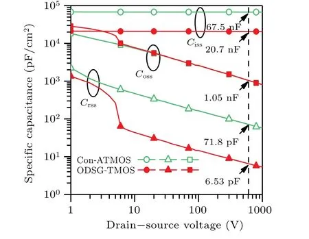
Figure 4 shows the dependence of the extractedCiss,Crss,and output capacitance (Coss) onVdsfor the two structures.It can be seen that asVdsincreases,Cissremains almost unchanged, whileCossandCrssshow obvious nonlinear characteristics.The two parameters for the proposed device at theVdsof about 5 V change suddenly,which is caused by the depletion of the heavily doped JFET layer.In theVdsrange from 0 V to 1000 V,theCissandCrssof the proposed ODSG-TMOS structure are both smaller than those of the Con-ATMOS structure.The values extracted at theVdsof 600 V are shown in Fig.4.At theVdsof 600 V, theCossof the two structures are almost the same, while theCissandCrssof the ODSGTMOS decrease by 69.3%and by an order of magnitude when compared to those of the Con-ATMOS,respectively.It can be concluded that the reduced gate depth as well as decoupled interaction between the gate and drain/source introduced by the DSG structure results in the improvement of theCissandCrss.TheCissandCrssfor a power switching device are of particular importance since it has a great influence on thePsw.Moreover,the smaller ratio ofCrsstoCissfor the proposed structure is of benefit to suppressing the false turn-on of the device.Considering that the capacitance characteristics at a certain terminal voltage cannot fully reflect the influence of the parasitic capacitance on the switching characteristic of a device,the gate charging characteristic is studied.Figure 5 shows the comparison of gate charging characteristic between the two structures.The test circuit is also shown in the inset.SmallerCissandCrssenable faster charging speed and also improve theQgdandQg.WithVgsin a range from 0 V to 15 V, theQgdandQgare 144 nC/cm2and 1330 nC/cm2for the Con-ATMOS,and 28 nC/cm2and 370 nC/cm2for the ODSG-TMOS, respectively.TheQgdandQgfor the ODSG-TMOS are reduced by 80.6% and 72.2% compared with those for Con-ATMOS,respectively.The high frequency figure of merit (HFFOM,Ron·Qgd) of the Con-ATMOS is 286.56 m?·nC while that of the ODSG-TMOS is only 47.32 m?·nC.In addition, another widely used HFFOM,theRon·Qg,is 2646.70 m?·nC for the Con-ATMOS and 625.30 m?·nC for the ODSG-TMOS.They are improved by 83.5%and 76.4%,respectively.To better demonstrate the advantage of the ODSG-TMOS, the HHFOMs of the reported devices are also compared.TheRon·QgdandRon·Qgfor the device in Ref.[14] are 438 m?·nC and 1722.8 m?·nC while those for the device proposed in Ref.[15]are 449 m?·nC and 2094 m?·nC, respectively.It is obvious that the performance of the ODSG-TMOS is improved significantly.
The switching waveforms with inductive load for the two devices are plotted in Fig.6(a).TheVgsis turned on att=0μs and turned off att=20 μs.It is obvious in Fig.6(a) that the Miller platform of the proposed ODSG-TMOS is significantly shortened,which is consistent with the result mentioned above.Owing to the reducedCissandCrss, the switching delay time of the ODSG-TMOS decreases significantly and the switching speed increases.The turn-on delay time and the turn-off delay time of the Con-ATMOS are 1.92μs and 3.24μs while those of the ODSG-TMOS are only 540 ns and 920 ns,they decreasing by 71.9% and 71.6%, respectively.In addition,power loss of the proposed ODSG-TMOS also decreases.The total power loss, including the conduction power loss(Pcon)andPswof the two structures at different frequencies are depicted in Fig.6(b).ThePconandPswof the ODSG-TMOS are 15.6%and 77.0%lower than those of the Con-ATMOS,respectively.As frequency increases,thePconremains constant,with the same duty cycle of 50%, but the difference inPswbecomes greater.Benefiting from the higher switching speed and lowerPsw, the ODSG-TMOS is more promising to high frequency applications than the Con-ATMOS.
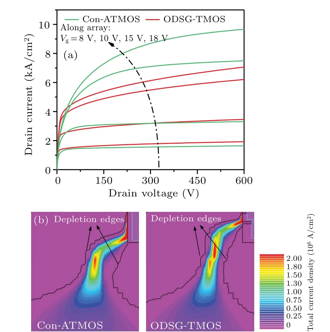
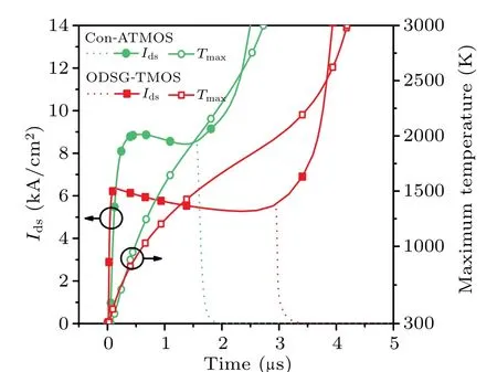
Figure 7(a)showsI–Vcharacteristic curves varying with drain voltage till saturation for the two structures under different values ofVgs.It can be seen that when theVgs=8 V and 10 V, the values ofId,satfor the Con-ATMO and the ODSGTMOS are almost the same.However, when theVgs=15 V and 18 V, the values ofId,satof the ODSG-TMOS are much smaller than those of the Con-ATMOS, owing to the lateral depletion effect provided by the lower SG under gate as shown in Fig.7(b).The black lines in the figures are depletion edges of the two structures at theVdsof 600 V withVgs=15 V.It is obvious that the depletion region of the ODSG-TMOS expands widely, thus reducing the width of electron conduction path.SmallerId,satconduces to reducing the power density when the device is under the short-circuit condition.Therefore,a longertscis obtained for the ODSG-TMOS as shown in Fig.8.For the SC simulation,aVgsof 15 V,a gate resistor of 1 ? and a bus voltage of 600 V with electrothermal coupling models are used.The dotted current curves represent the critical time at which the devices can be turned off normally.On the contrary, the solid current curves refer to the case where the devices fail in a longer short-circuit operation time.It can be seen that thetscis 1.6 μs for the Con-ATMOS and 3.0 μs for the ODSG-TMOS.It is improved by 87.5%,with theId,satreduced.Once the two MOSFETs are turned on,their SC currents rapidly increase and reach the corresponding values ofId,sat.After that, the saturation currents of the two structures start to decrease owing to the self-heating effect as well as reduced carrier mobility in the inversion MOS channel and drift region with the increase of junction temperature.Owing to the large power loss under the SC condition,once the junction temperature reaches the intrinsic temperature limit, the current increases rapidly and then thermal runaway occurs.
To evaluate the reverse-biased SOA(RBSOA)of the proposed device, the large-current turn-off capability with an inductive load is discussed in Fig.9.In the simulation,an initial junction temperature of 448 K, a bus voltage of 1200 V and a large current of 1800 A (6 times the nominal current) are used, with the electro-thermal coupling model adopted.The values ofVgsof the two devices both turn from 15 V to 0 V att=2μs.After a delay of a few microseconds,the ODSGTMOS is normally turned off while the Con-ATMOS cannot.It can be found that for the Con-ATMOS,after theVdsreaches the bus voltage of 1200 V,theIdsstarts to drop normally.However, after a short drop, theIdsrecovers to 1800 A again and theVdsof the Con-ATMOS starts to drop.The Con-ATMOS fails in the large-current turn-off process and losses blocking capability.The junction temperatures of the two devices in the turn-off process are also shown in the figure.It is found that the junction temperature of the Con-ATMOS increases to about 2000 K while the proposed ODSG-TMOS shows much less temperature rise.Like the results shown in Fig.6, the slower turn-off speed and higherPswfor the Con-ATMOS contribute to the rapid rise of the junction temperature.
The influence of the fin-shaped control gate width (Wf)on the performance of the ODSG-TMOS at 50 kHz is shown in Fig.10.In the simulation,the fin-shaped source-connected SG keeps the width identical with that of the fin-shaped gate.It can be seen in Fig.10(a)that theCgdkeeps almost unchanged owing to good shielding effect provided by the lower SG while theCgssignificantly increases as theWfincreases from 0.1μm to 0.4 μm.Accordingly, theQgdshown in Fig.10(b) keeps almost unchanged while theQgandPswincrease withWfincreasing.The smaller theWf, the better performance can be obtained.Further research results show that the smallerWfnot only reduces the overlapping area between the gate and lower SG, but also increases the thickness of the oxide layer between the fin-shaped gate and the fin-shaped source-connected SG,which both decouple the interaction between the gate and source,and therefore,significantly reducing theCgsof the device.It shows that theCgsaffects not only the switching speed but also the switching power loss, especially when theCgdis small enough.

Figures 11(a) and 11(b) show the relationship betweenId,satandRon,sp,and the relationship between BFOM andNJFfor different values of JFET layer width(WJF),respectively.It can be seen from Fig.11(a)that with the sameWJF,theRon,spdecreases andId,satincreases with the increase of theNJF.Similarly,theRon,spdecreases andId,satincreases with the increase of theWJFwhen theNJFis kept unchanged.The reason is that increasingNJFand/orWJFof the JFET layer provides a low resistance path for electrons in the conduction state at lowerVdsregime.However,the JFET effect provided by the lower SG at largeVdsis also attenuated since the JFET layer is more difficult to deplete.Figure 11(b)shows the influence of theWJFandNJFon the Baliga’s figure of merit(BFOM,BV2/Ron,sp)for the proposed device.As mentioned above,the blocking capability of the device is determined by the lower one of theBVavandBVox.When theNJFis low, theBVavis a lower one and the BFOM increases as theNJFincreases,owing toRon,spdecreasing.However,theBVoxdecreases rapidly with the increase ofNJF,owing toEox,peakincreasing in the trench corner.TheBVoxbecomes lower thanBVavwhen theNJFis greater than a certain value.And after that, the BFOM decreases rapidly with the increase ofNJF,owing to theBVoxdecreasing.Therefore,considering the influence of theWJFandNJF, there appears a balance after the conduction performance,BFOM and SCSOA for the proposed ODSG-TMOS have been optimized.
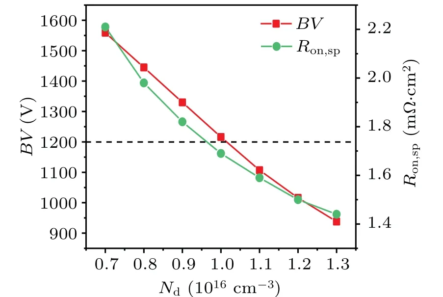
Figure 12 shows the influence of concentration of the Ndrift region (Nd) on theBVandRon,sp, respectively.As expected,the two parameters both decrease with the increase ofNd.WhenNdincreases from 7×1015cm-3to 1.3×1016cm-3,BVdecreases from 1559 V to 938 V andRon,spdeclines from 2.21 m?·cm2to 1.44 m?·cm2.It can be found that to ensure that theBVis larger than 1200 V,theNdmust be kept less than or equal to 1×1016cm-3.Therefore, the optimizedRon,spis obtained when theNdis equal to 1×1016cm-3.In this case,theBVof the ODSG-TMOS is almost the same as that of the Con-ATMOS while theRon,spis 15.1%lower.
In order to show the feasibility of the proposed ODSGTMOS structure, a possible manufacturing process flowchart is shown in Fig.13.Firstly,an epitaxial lightly doped N-drift layer is grown on an N+substrate.After forming the epitaxial layer, the P+SLD, N+source region and P-base form via multiple ion implantation as shown in Fig.13(b).After the gate trench is etched, an L-shaped JFET area forms through tilted multiple ion implantation as shown in Figs.13(c)–13(d).Using thermal oxidation to form an oxide layer on the surface and the bottom and sidewalls of the trench, the gate trench is filled with polysilicon and then etched to form the lower split gate as shown in Figs.13(e)–13(g).Similarly, the fin-shaped gate and source also form by filling and etching process as shown in Figs.13(h)–13(j).[14,15]The process of forming finshaped gate is a self-aligned process andWfis determined by the deposited thickness of the polysilicon film and subsequent etching process.After that, dielectric is deposited and metal process is utilized to form the source and drain electrode.The final structure fabricated is shown in Fig.13(l).

4.Conclusions
A novel SiC ODSG-TMOS structure is proposed and investigated in this work.Comparing with the Con-ATMOS,BVavkeeps almost unchanged while theEox,peakbecomes 3.29 MV/cm for the Con-ATMOS, and 2.94 MV/cm for the proposed ODSG-TMOS, which improves theBVoxand gate oxide reliability.And theRon,spis also improved by 15.1%due to the introduction of the highly doped JFET layer.More importantly,compared with the Con-ATMOS,the ODSG-TMOS shows high dynamic performance and improved SOA capability.TheCissandCrssof the ODSG-TMOS decrease by 69.3%and by an order of magnitude when compared to those of the Con-ATMOS, respectively.The value ofQgdandQgare reduced by 80.6%and 72.2%, respectively.Therefore, the HFFOM ofRon,sp·QgdandRon,sp·Qgfor the proposed ODSGTMOS are improved by 83.5%and 76.4%, respectively.ThePswof the proposed ODSG-TMOS is 77.0% lower than that of the Con-ATMOS.In addition,the SCSOA and RBSOA are also improved.With a significantly reducedId,sat, thetscis 87.5%longer than that of the Con-ATMOS at theVgof 15 V.The ODSG-TMOS can be normally turned off under a bus voltage of 1200 V and a large current of 1800 A while the Con-ATMOS fails in the turn-off process.The key parameters that have a strong influence on performance of the ODSG-TMOS are discussed,which presents a further improvement direction for the proposed structure.Considering the improved switching performance and enhanced SOA, the ODSG-TMOS is a promising candidate for high-frequency and high-power applications.
Acknowledgement
Project supported by the China Postdoctoral Science Foundation(Grant No.2020M682607).
猜你喜歡
瘋狂英語(yǔ)·初中天地(2023年7期)2023-08-18 05:01:35
Plasma Science and Technology(2022年8期)2022-09-14 08:18:00
意林彩版(2022年1期)2022-05-03 10:25:07
Chinese Physics B(2022年4期)2022-04-12 03:48:20
攝影與攝像(2020年11期)2020-09-10 07:22:44
武漢科技大學(xué)學(xué)報(bào)(社會(huì)科學(xué)版)(2020年2期)2020-04-28 01:54:38
赤水源(2018年6期)2018-12-06 08:38:10
河北醫(yī)科大學(xué)學(xué)報(bào)(2017年2期)2017-03-10 02:50:07
Transactions of Nanjing University of Aeronautics and Astronautics(2015年1期)2015-11-21 07:08:56
科學(xué)中國(guó)人(2015年22期)2015-02-28 09:14:37

- Chinese Physics B的其它文章
- The application of quantum coherence as a resource
- Special breathing structures induced by bright solitons collision in a binary dipolar Bose–Einstein condensates
- Effect of short-term plasticity on working memory
- Directional-to-random transition of cell cluster migration
- Effect of mono-/divalent metal ions on the conductivity characteristics of DNA solutions transferring through a microfluidic channel
- Off-diagonal approach to the exact solution of quantum integrable systems