
Bottom-up approaches to microLEDs emitting red,green and blue light based on GaN nanowires and relaxed InGaN platelets
2023-02-20 13:16:28ZhaoxiaBi畢朝霞AndersGustafssonandLarsSamuelson
Chinese Physics B 2023年1期
關(guān)鍵詞:朝霞
Zhaoxia Bi(畢朝霞), Anders Gustafsson, and Lars Samuelson
Division of Solid State Physics and NanoLund,Lund University,Box 118,SE-221 00 Lund,Sweden
Keywords: microLEDs,RGB,GaN,InGaN
1. Introduction
While highly efficient nitride light-emitting diodes(LEDs), with device sizes on a scale of several hundred micrometers,have been widely applied for general lighting,there are needs to reduce the LED size for new applications.[1–7]Mini-LEDs,with a size of about 100–200 μm,are suitable for backlighting of liquid crystal displays(LCD)with a high contrast ratio and excellent high dynamic range.[3,4]With further miniaturization, microLEDs have an extension below 50 μm,and can be used as individual pixels for the next generation self-emissive displays.[1–4]Compared with LCD and organic LED displays, microLEDs provide higher brightness, contrast ratio and resolution,faster response,longer lifetime,better environmental stability and wider viewing angles. Besides self-emissive displays,microLEDs are also attractive for other applications, such as visible light communication, optogenetics, bio-imaging and sensors.[5–7]Nitride microLEDs were firstly introduced by Jiang’s group in 2000,[8]and a 10×10 pixel microdisplay based on blue nitride microLEDs was presented by this group in 2001.[9]From then on,many research groups and companies have been working on this area,covering epitaxy,[10–15]device fabrication[4,6,16,17]and display manufacturing.[9,18–20]In 2014,Apple entered this area by acquiring LuxVue, a company founded in 2009 for microLED displays based on pick-and-place technology. About this time,GLO AB, a spin-off from our research group, switched the strategy from large area LEDs to microLEDs based on GaN nanowires(NWs). Recently,Google acquired Raxium for the technology of monolithic integration of red, green and blue(RGB) microLEDs by epitaxy, instead of using the challenging mass transfer for the microLED display manufacturing.
There are challenges to fabricate microLEDs.In the common top-down approach,where mesas of microLEDs are obtained through dry etching of a planar LED wafer, side wall damage is a well-known issue,creating non-radiative recombination centers and leakage current path.[4,21,22]For large area LEDs, the side wall damage does not affect the LED performance,or the influence is negligible as the side walls are only a small fraction of the entire device area.However,for most of microLED displays(including televisions of 4K and 8K,augmented/mixed reality glasses and head-up displays), the device size needs to be smaller than 15 μm. In this size range,side wall damage affects the device performance significantly due to the increased perimeter/surface ratio of the microLEDs.Besides the reduced external quantum efficiency (EQE), the current density for the peak EQE increases, which is unfavorable for microLED displays.[21,22]It was reported that the surface damage can be reduced by chemical treatments and side wall passivation for microLEDs of 10 μm and above.[4]Wanget al. developed neutral beam etching for microLED fabrication with reduced side wall damage,and fabricated devices which showed constant EQE with the device size down to 6 μm.[16]
Planar nitride LED wafers consist of a GaN layer on a foreign substrate. The layers have a high density of threading dislocations, typically 108cm-2on sapphire substrates and>109cm-2on Si substrates. Large area LEDs statistically include similar numbers of dislocations,which means that the LED variation caused by dislocations is negligible. This may not be true for LEDs at sizes of several micrometers, and individual microLEDs may include different numbers of dislocations. The dislocations usually end with V-pits at the wafer surface with a diameter of 100–200 nm.[23]This obviously affects the uniformity of microLEDs and brings complexity to the display manufacturing.
MicroLEDs are used as self-emissive pixels for displays.Individual pixels need to include three microLEDs emitting RGB light to realize full color displays. Nitride microLEDs are normally chosen for the blue and green emissions. It is desirable to also base the red microLEDs on nitride materials,rather than AlInGaP. Red nitride microLEDs are expected to out-perform the AlInGaP ones due to significantly higher surface recombination rate and longer carrier diffusion lengths of the latter.[10]The best wall plug efficiency of 16.8% was reported recently for large area nitride red LEDs by Jiang’s group on Si substrates.[23]However, this is still much lower than the efficiencies of nitride blue and green LEDs. For nitride red microLEDs, the EQE is currently still below 10%.The major reason for this low efficiency of nitride red LEDs is the increasing lattice mismatch between InGaN quantum wells(QWs)and GaN templates. In contrast to the InGaN QWs for blue and green emissions where respective indium contents are about 15%and 25%,the indium content needs to be more than 35%for red light emission. The increased strain can introduce new dislocations and lead to serious quantum-confined Stark effect,resulting in a low device efficiency of nitride red LEDs.Replacement of GaN templates with InGaN should be a solution to this issue,[12,24,25]but high quality InGaN planar templates are still not available due to growth challenges arising from the differences between GaN and InN.For instance,the large difference in the interatomic spacing results in a solid phase miscibility gap, and the much higher vapor pressure of InN as compared to that of GaN leads to a low indium incorporation in the InGaN alloy.[26]
In this paper, we review our efforts to microLEDs from the material perspective. We have used two separate approaches, basing the microLEDs on GaN NWs or InGaN platelets. Both approaches are based on selective area growth of sub-micrometer LED structures, which can be used as building blocks to assemble microLEDs with different sizes.With these bottom-up approaches,the subsequent dry etching to define the device area can be aligned so that the side walls of the mesa do not include any LED structures and side wall damage can be avoided. Another benefit is that such structures are grown virtually free from dislocations, which eliminates the possible uniformity issue to microLEDs caused by dislocations for the top-down approach as discussed above. Furthermore, the InxGa1-xN platelets offer a smooth top c-plane for the InyGa1-yN QW growth(x <y). This makes it possible to grow green and red InGaN QWs with a similarly low-level of strain as the blue-emitting InGaN QWs on GaN templates.This is expected to be an excellent solution for highly efficient green and red microLEDs.
2. Methods
All the structures in this paper were grown with selective area metal–organic vapor phase epitaxy (MOVPE). Triethylgallium(TEG)and trimethylindium(TMI)were used as the gallium and indium precursors, and the nitrogen precursor was NH3. (0001)GaN films grown on sapphire,SiC or Si substrates were used as templates(Fig.1(a)),on top of which a layer of stoichiometric Si3N4was deposited by low pressure chemical vapor deposition. The Si3N4layer was 30–100 nm thick and used as a growth mask for the subsequent nitride growth. Electron-beam lithography or nano-imprint lithography was used to pattern the Si3N4mask with hexagonal arrays of openings which had a diameter of 100–200 nm, as shown in Fig. 1(b). Due to the growth selectivity of nitrides, the growth takes place only on the GaN surface in the openings,without any nucleation on the Si3N4mask. In this way, arrays of nanometer-sized structures can be grown,such as GaN nanowires(NWs)as shown in Fig.1(c)and InGaN pyramids as shown in Fig.1(d).
The GaN NWs have six vertical (10ˉ10) m-planes as the side facets, in contrast to the six inclined (10ˉ11)s-planes for the InGaN pyramids. The shape of the structures depends on growth rates of m-, s- and top (0001) c-planes, as shown in Fig. 1(e). The inclined s-planes are N-terminated.[27]Under common MOVPE growth conditions(NH3-rich),the nitrogen atoms at the s-plane surface tend to be passivated by hydrogen through formation of N–H bonds. This prevents the Ga adsorption on s-planes, leading to an extremely low growth rate of s-planes,[27]much lower than the growth on m- and c-planes. As a result, the areas of m- and c-planes shrink with continued growth, while the s-planes expand and lead the structure shape to a final pyramid, according to the kinetic Wulff’s plot.[28,29]According to this, the growth rate of s-planes has to be enhanced by changing growth conditions to obtain the NW growth fashion with vertical m-plane side facets. The key to NW growth is to grow under a metal-rich condition,and this will be discussed in next section.
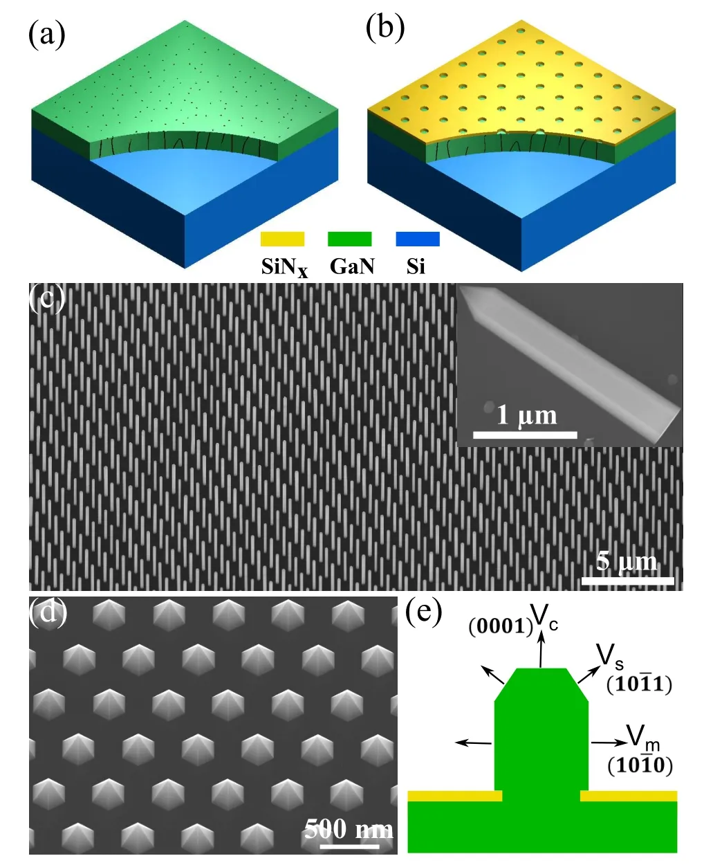
Fig.1. Selective area MOVPE growth of GaN NWs and InGaN pyramids.(a) A schematic of a GaN layer on a Si (111) substrate with dislocations indicated by dark vertical lines. (b)A schematic of template preparation on GaN/Si with a Si3N4 mask patterned with 100–200 nm diameter circular openings. (c)and(d)Arrays of GaN NWs and InGaN pyramids grown on the patterned templates shown in(b). The SEM images were recorded with a 30° tilt of the samples. Inset in(c)is a side view SEM image of a single GaN NW after GaN shell growth. This NW was pushed over and laid on the substrate surface for side view imaging. (e)A schematic showing three crystal planes of m-, s- and c-planes and their grow rates determining the structure shape according to the kinetic Wulff’s plot.[28] (a)and(b)Reproduced with permission from Ref.[36]. Copyright 2019 American Chemical Society.
3. GaN NWs and core/shell LEDs
NH3is a commonly used nitrogen precursor for MOVPE growth of nitride semiconductors. Due to the low efficiency of NH3cracking, a high V/III ratio, typically a few thousand, is used for the nitride growth. The active hydrogen species from the NH3decomposition can bond with nitrogen atoms on the s-plane surface, and then lead to the extremely slow growth on s-planes. To avoid such surface reconstruction and obtain the GaN NW growth fashion,two growth methods have been used. One is to use the pulsed growth mode,[30–32]where the NH3and Ga precursor flow into the reactor alternatively. By tuning the pulse and interruption durations, GaN NWs with six vertical m-plane side facets can be realized. The NW top ends with either only six s-planes or s-planes plus a small top c-plane. In this case, it is obvious that s-planes grow much faster so that m-planes appear as the side facets. The other method is to keep the continuous supplies of the NH3and Ga precursor, but with a V/III ratio which is usually two orders of magnitude lower than those used for planar GaN MOVPE growth.[33–35]We have been focusing on the method of the latter for Ga-polar GaN NWs. With such a low V/III ratio, the GaN growth is initiated in the openings with (10ˉ13) planes at the top. The growth develops into (10ˉ12) once it grows out of the openings in the mask. As the growth continues,many tiny crystal planes are formed at the NW top, leading to growth mainly in the axial direction with limited deposition on the vertical m-planes.[36]After the NW growth, a radial GaN shell can be grown by increasing the NH3flow rate.With the increased V/III ratio,s-planes are formed at the NW top, which enhances the shell growth on the m-planes due to the slow growth on s-planes. Figure 1(c)shows arrays of GaN NWs with a diameter of about 180 nm.The inset shows a GaN NW after growth of an 80 nm-thick GaN shell, resulting in a total diameter of about 340 nm. The NW top shows a pyramid delimited by six s-planes,formed during the shell growth.
As mentioned above, planar GaN layers on foreign substrates have a high density of threading dislocations. For the selective area growth, most of the dislocations from the underlying GaN layers are blocked by the growth mask, simply from a statistical point of view. However, there may still be dislocations which appear in the openings and then enter the GaN NWs.[29,36]The dislocations,entering the GaN NWs,tend to bend into c-planes in the bottom part of the GaN NWs and terminate at one of the m-planes as shown by the transmission electron microscopy (TEM) image in Fig. 2(b). The m-plane side facet, terminating the dislocation, grows much faster than the other side facet free from dislocations, leading to growth of asymmetric, but still hexagonal GaN NW.One example of such asymmetric NWs is shown in the topview scanning electron microscopy(SEM)image in Fig.2(a),marked in the red circle. Seven GaN NWs with such an asymmetric shape were characterized with TEM and this behavior of dislocation propagation was observed in all of them.For the GaN NWs with a symmetric hexagonal shape, no dislocation was found as shown by the TEM image in Fig.2(c). To reduce the dislocation propagation into GaN NWs, openings smaller than 100 nm are preferable. Meanwhile,a thick growth mask can also be used to enhance the probability of the dislocation bending before GaN grows out of the openings. Another way is to form a void under the openings by thermal annealing of the patterned templates so that dislocations can be annihilated before entering the GaN NWs.[37]With all these methods applied,uniform GaN NWs as shown in Fig.1(c)were realized on GaN/Si substrates with a pattern size of 1.5×3 mm, free from asymmetric NWs caused by dislocations.
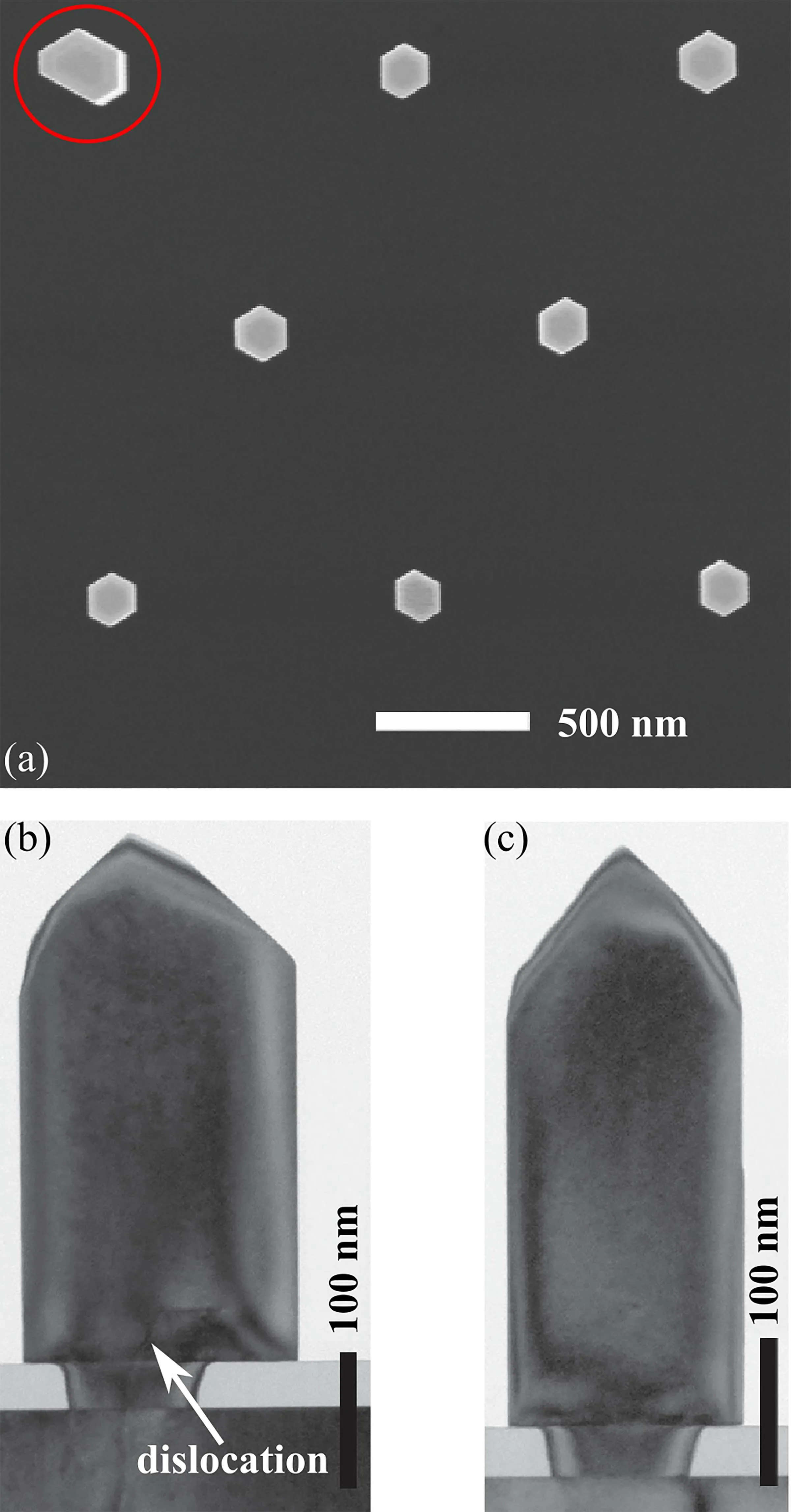
Fig.2. Shape regularity of GaN NWs and bending of dislocations propagated from underlying GaN layer. (a)A top-view SEM image of GaN NWs.A GaN NW with an asymmetric shape is shown in the red circle. (b) and(c) Cross-sectional TEM images of GaN NWs with asymmetric and symmetric shapes, respectively. Reproduced with permission from Ref. [36].Copyright 2019 American Chemical Society.
GaN NWs have six m-plane side facets for InGaN QW growth. Before the growth, a GaN shell was grown for a high quality and meanwhile a large surface area for the In-GaN QWs. The inset in Fig. 1(c) is an example of GaN NWs after the shell growth,showing smooth m-plane surfaces.InGaN QWs grow mainly on the m-plane side facets due to high V/III ratios,as discussed above for the GaN shell growth.Figure 3 shows TEM characterization of an InGaN single QW grown on a GaN NW.The InGaN QW was capped by an outer GaN shell. The high resolution TEM images, recorded from different regions of the NW, show a varied thickness of the InGaN QW. The thickness increases from 4.0 nm at the NW base to 4.7 nm in the NW middle. The thickness increases further to 8.8 nm at the transition to the inclined s-plane. The low growth rate on the s-plane can be clearly seen with a QW thickness of about 0.5 nm. During the selective area growth,the gallium and indium species, landing on the growth mask,diffuse on the mask and reach the nearest NWs. Such gallium and indium species also diffuse along the side facets of NWs and contribute to the growth of the InGaN QW. Due to the slow growth on the s-planes, the gallium and indium species might accumulate at the NW top and form a local region with high concentrations of gallium and indium species. This can result in a concentration gradient along the NWs, leading to the thickness variation of the InGaN QW as shown in Fig. 3.Besides the thickness variation,the indium content is found to increase from 7% at the NW base to 17% at the NW top for the sample in Fig. 3, according to the data of energy dispersive x-ray spectroscopy(EDS).The large discrepancy may be over-estimated considering the inaccurate EDS measurement on the thin QW at the NW base due to the limited spatial resolution. However, the distribution of the indium content is consistent with the thickness variation along the m-plane. To enhance the uniformities of the thickness and the indium content of the QW, short GaN NWs are preferable as shown in Ref.[38]. However,the thicker QW developing locally at the transition area between the m- and s-planes seems unavoidable. Its influence on the LED devices can be reduced during device fabrication by plasma passivation or etching.[38]

Fig.3. TEM characterization of an InGaN QW grown on the side facets of a GaN NW.(a)An overview scanning TEM image. The InGaN QW can be observed in this image as two white lines on both sides of the NW. Highresolution TEM images of(b), (c)and(d)were recorded at three locations marked in(a),from the top to the base of the NW.
After InGaN QW growth,a p-AlGaN shell was grown as an electron blocking layer, which was followed by a p-GaN shell to create a complete LED structure(Figs.4(a)and 4(b)).The GaN NW and the GaN shell before InGaN QW growth were doped with Si. In this architecture, each NW works as an individual LED, which can be used as building blocks to assemble microLEDs and large area LEDs. A fabricated multi-NW LED was cleaved with some NWs cracked through the center, as shown in Fig. 4(b). Each individual layer can be seen, including the ITO contact to the outer p-GaN shell.The n-contact was made to the underlying Si-doped n-GaN layer. Figure 4(c)shows the current–voltage characteristic of a green NW LED, exhibiting low shunt leakage down to the nano-Ampere current range. Green NW microLEDs were fabricated with sizes of 5×5 μm2,10×10 μm2and 20×20 μm2,in parallel to microLEDs based on planar green LED wafers.Figure 4(d) shows the EQE comparison between microLEDs made from NWs and planar LED wafers. The microLEDs made from planar LED wafers suffer from the damage by dry etching,leading to a reduced EQE from the 20×20 μm2microLED to the one of 10×10 μm2. For the same reason, the EQEs were much lower than those of the large area LEDs fabricated from the planar LED wafers. NW microLEDs also need dry etching to fabricate device mesas, but dry etching does not hit any individual NW structures. This is the reason why NW microLEDs in Fig.4(d)show consistent EQE curves,regardless of the device size. In addition, figure 4(d) shows that the EQE of NW microLEDs peaks at very low current densities of 0.1–0.2 A/cm2,while the microLEDs from planar LED wafers show efficiency peaks at tens of A/cm2. This is a favoring feature of NW microLEDs for the display applications that use low temperature polycrystalline silicon (LTPS)thin film transistors made on glass,since the LTPS technology has a difficulty delivering high currents to each subpixel. Figures 4(e)and 4(f)show examples of arrays of blue and green NW microLEDs with a size of 30×30 μm2.
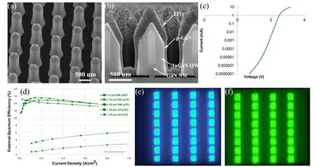
Fig.4. Fabrication of GaN NW LEDs and electrical characterization. (a) Arrays of GaN NW LEDs. The sample was tilted by 30° for this SEM image. (b)An SEM image showing the cross-section of a processed GaN NW LED.(c)Current–voltage characteristic of a green NW LED showing low shunt leakage. (d)EQE curves of green NW microLEDs,in comparison with green microLEDs made from planar LED wafers,at sizes from ranging 5×5 μm2 to 20×20 μm2. (e)and(f)Optical microscopy images of blue and green NW microLEDs with a size of 30×30 μm2. (a)and(c)Reproduced with permission from Ref.[35]. Copyright 2016 Elsevier. (d)Reproduced with permission from Ref.[2]. Copyright 2021 Elsevier.
4. InGaN platelets and RGB microLEDs
Based on GaN NWs,blue and green microLEDs were realized. However, it may be difficult to extend emissions to the red color with a decent efficiency due to the increased lattice mismatch between the red-emitting InGaN QWs and GaN NW templates. We attempted to grow InGaN NWs to serve as a template for red InGaN QWs to reduce the lattice-mismatch strain. However, it was found that the InGaN NW growth in our case was not achievable and the growth resulted in a pyramid shape.The reason is the much higher equilibrium nitrogen pressure for InN as compared to the one for GaN,which means that the incorporation of indium into GaN requires a high V/III ratio. With the low V/III needed for the selective area growth of GaN NWs,indium cannot get incorporated and only forms droplets. The high V/III ratio makes the s-planes dominate the structure shape and leads to the growth of InGaN pyramids,instead of NWs, as discussed above. Figure 1(d)shows typical InGaN pyramids grown from 100–200 nm large openings.To ensure the growth of uniform InGaN pyramids and avoid the dislocation propagation from the underlying GaN layer, a GaN seed was grown using the conditions for GaN NWs. This GaN seed only fills up the opening as shown in Fig.5(a),with an ultra-small pyramid top sticking out of the opening.
For the InGaN pyramid growth in Fig.5(a),five thin GaN marker layers were inserted to observe the evolution of the shape during the growth. (10ˉ12) and (10ˉ13) planes, constituting the top pyramid of the GaN seed, tend to develop into s-planes of(10ˉ11)after the InGaN growth starts.[39]This leads to the formation of a top c-plane, shown by the first GaN marker layer. As the growth continues, the c-plane size shrinks,and the s-planes expand,which makes the structure a complete pyramid before the growth of the fifth GaN marker layer.The GaN marker layers on the s-planes are almost invisible due to the slow growth.The growth was studied with varying the opening diameter and the pitch. As shown in Fig.5(b),the pyramid volume increases linearly with the collection area,which is the reciprocal of the opening/pyramid density, indicating diffusion-controlled growth for a pitch up to 2 μm.This means that the gallium and indium species, landing on the growth mask, diffuse to the nearest pyramids and contribute to the growth of the pyramids. It was found that the indium contents in the InGaN pyramids can be increased by raising the growth rates, shifting photoluminescence (PL) peak from 390 nm to 480 nm as shown by Fig. 5(c). The corresponding indium contents increase from about 5%to 18%. The In-GaN pyramids in our current study usually have a diagonal size of 800 nm at the base. Figure 5(b)shows that the InGaN pyramids can be grown up to 2 μm or larger without parasitic growth on the Si3N4mask. However,the growth of larger InGaN pyramids can result in a large variation of the indium content in the pyramids due to the increased surface area (or decreased growth rate along the facet direction).
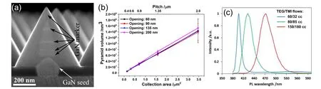
Fig.5. Selective area growth of InGaN pyramids. (a)A cross-sectional SEM image of an InGaN pyramid. Five thin GaN marker layers were inserted during growth to observe the growth evolution. (b) InGaN pyramid volume dependence on the collection area with varied opening size, with the corresponding pitch shown in the top x-axis. (c)PL spectra of InGaN pyramids grown with different growth rates. (a)and(b)Reproduced with permission from Ref.[39].Copyright 2018 AIP Publishing.
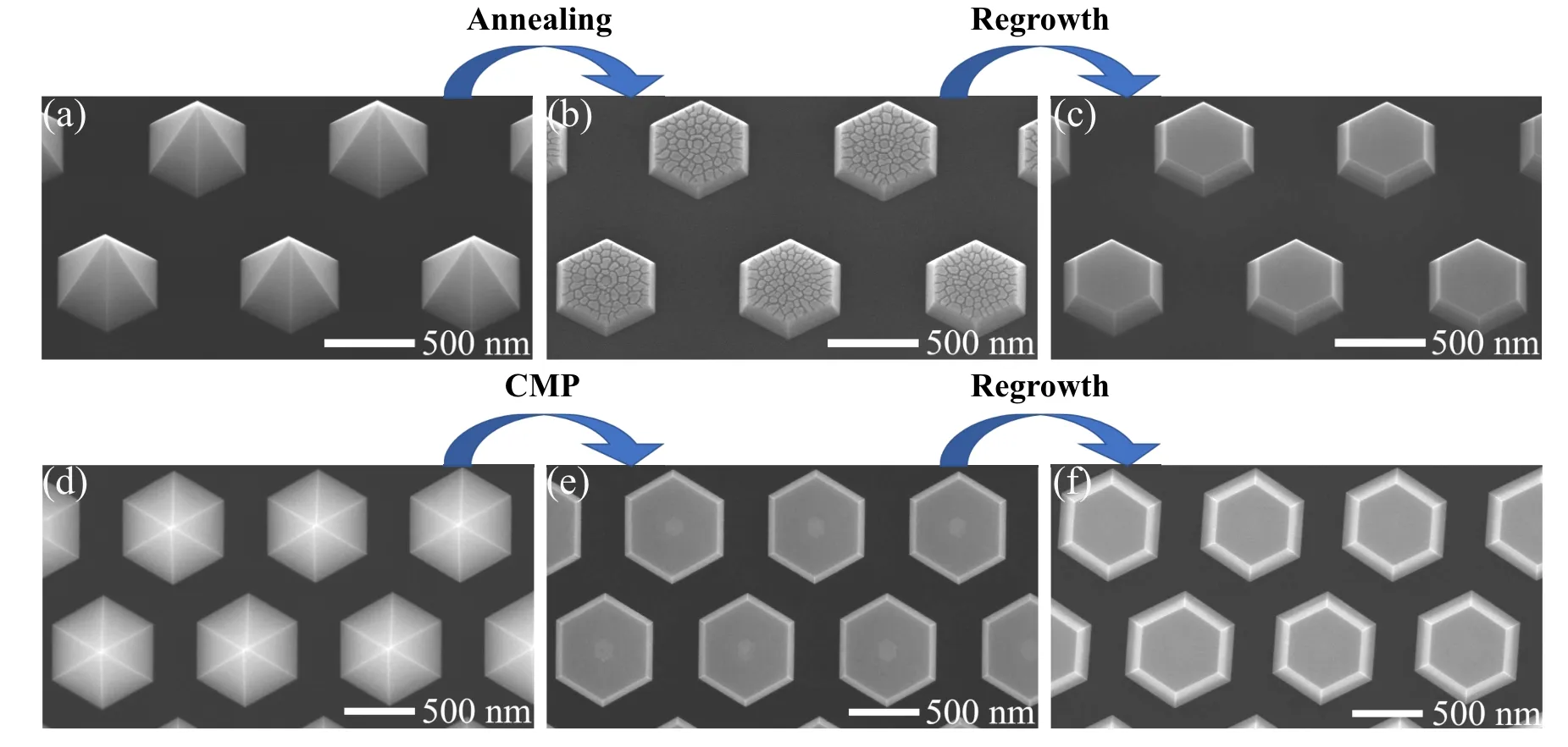
Fig.6. Procedures to grow InGaN platelets by truncating InGaN pyramids through either high temperature annealing(shown in top row(a)–(c))or CMP(shown in bottom row(d)–(f)). (a)–(c)Reproduced with permission from Ref.[15]. Copyright 2019 American Chemical Society.
The InGaN pyramids were truncated from the apex to obtain a top c-plane for the subsequent growth of InGaN QWs,as shown in Fig. 6. We have used two different approaches to achieve the flat platelets, either high temperature annealing or chemical mechanical polishing (CMP).[15,40,41]The high temperature annealing under NH3protection etches the pyramids from the top apex, while the inclined s-planes stay intact. Annealing for several minutes can result in a thin structure (<100 nm in thickness) as shown in the SEM image in Fig.6(b). The top c-plane surface is rough with grains due to the InGaN decomposition. InGaN regrowth was conducted to obtain a platelet structure with a smooth top c-plane,as shown by Fig. 6(c). In this case, an InGaN intermediate layer must be grown first with a low indium content(about 5%)to flatten the rough c-plane, followed by the growth of a high-quality top layer with the identical indium content as the original In-GaN pyramids. The InGaN intermediate layer always has the indium content of about 5%,irrespective of the indium content in the InGaN pyramids. Due to the lattice mismatch, this intermediate layer leads to dislocation formation for the growth of InGaN platelets with an identical content of 18%.[15]As an alternative, CMP was used to truncate the InGaN pyramids, as shown by the SEM image in Fig. 6(e). A smooth surface was produced by CMP, in contrast to the rough surface obtained by the thermal annealing. In this way, InGaN regrowth can be conducted directly with an identical indium content as the original InGaN pyramids, leading to platelet structures completely free from dislocations. With both methods, high quality InGaN platelets with indium contents up to 18%can be fabricated with only single bilayer steps on the top c-plane.[15,40]As 18% is the target composition, we have to date not gone beyond 18%. The PL spectra measured at room temperature show full-widths at half-maximum (FWHMs) of 16 nm at 420 nm emission and 25 nm at 480 nm emission. As 18%is the target,we have not investigated the limit of indium content,but we are confident that it could be increased without any detrimental effects.
The color contrast between the top and the bottom layers visible on the side facets in Figs.6(c)and 6(e)shows that the InGaN regrowth mainly takes place on the top c-plane and the growth on s-planes is negligible. With continued growth,the c-plane size shrinks,and a full pyramid can be developed.A sample was grown with a 200–300 nm thick regrown In-GaN layer, leaving a small top c-plane. The structures were cleaved through and characterized with cathodoluminescence at room temperature (see the supplementary information in Ref.[40]). Spot mode cathodoluminescence spectra measured on the cleaved surface showed a peak variation of 4–5 nm for an average emission at 420 nm. This small peak variation indicates a good uniformity of the indium content(<1%)in the InGaN platelets. Such a high uniformity is needed for the subsequent InGaN QW growth. This sample also showed a large PL intensity boost,which is more than one order of magnitude higher as compared with the PL intensity from the original InGaN pyramids. Since the structure volumes of these two samples are similar,the PL intensity boost is explained by the growth dependence on s- and c-planes, where the growth on the c-plane has much less impurity incorporation than on the s-planes. We also found that the InGaN pyramid growth is much more sensitive to the reactor status than the planar LED growth on c-plane.
Figure 7(a)shows a schematic of the LED structure based on InGaN platelets. Thanks to the negligible growth on the splanes,a vertical p–i–n LED structure can be realized proceeding with growth on the c-plane. Both multiple QWs and single QW can be grown on the top c-plane of the InGaN platelets.Figure 7(b) shows a scanning TEM image of blue multiple QWs grown on a GaN platelet. Before the growth of the top seven blue QWs, three thinner QWs with an indium content of<10% were grown first. In this case, the GaN platelet was obtained by thermal annealing of a GaN pyramid.[29]The pyramid was formed by growing a GaN shell on GaN NWs,with negligible axial growth. With the GaN shell grown long enough, the s-planes will dominate the final structure shape,leading to the formation of full GaN pyramids. The size of the GaN pyramids depends on the height of the original GaN NWs. A longer NW will result in a larger pyramid when the entire m-planes are covered by s-planes.

Fig.7. InGaN QW growth on the top c-plane of InGaN platelets. (a) A schematic of the vertical p–i–n LED structure with a single InGaN QW grown on InGaN platelets. (b)and(c)Cross-sectional TEM images of blue multiple QWs grown on a GaN platelet and green single QW grown on an In0.10Ga0.90N platelet,respectively.Red single QW grown on In0.18Ga0.82N platelets is similar as the green one in(c). (d)Room-temperature PL spectra of blue,green and red single QWs grown on platelets of GaN,In0.10Ga0.90N and In0.18Ga0.82N.(a)and(c)Reproduced with permission from Ref.[15].Copyright 2019 American.
For green and red emissions, single InGaN QWs were grown on the top c-plane of InGaN platelets. Platelets of In0.10Ga0.90N and In0.18Ga0.82N were used for green and red InGaN QWs,respectively. Figure 7(c)shows the green InGaN QW grown on In0.10Ga0.90N platelets. The red InGaN QW grown on In0.18Ga0.82N platelets is similar and not shown here.In this way,the green and red QWs have a low-level strain similar to that of blue InGaN QWs grown on GaN layers,leading to reduced quantum-confined Stark effect and improved material quality. The strain between the underlying GaN layer and the InGaN platelet is accommodated by the small footprint in the mask opening. The platelet in Fig. 7(c) was obtained by thermal annealing and the InGaN intermediate layer is clearly seen in the middle of the structure (the layer with slightly darker contrast). The magnified image shows that the QW becomes thinner and completely disappears when approaching the inclined s-plane. Meanwhile, the QW is capped on the splane with a thin layer formed during the top barrier growth.These two features may effectively offer a self-assembly of a surface passivation of the QW. Figure 7(d) shows PL spectra of RGB InGaN QWs grown on InGaN and GaN platelets.For the green and red QW samples,the emissions from InGaN platelets are also seen in the short wavelength side together with the major green and red peaks from QWs. The FWHMs are 23 nm,37 nm and 51 nm for the blue,green and red emissions from QWs.
Blue LEDs based on single GaN platelet structures were fabricated with electron-beam lithography as shown in Fig.8(a), where the in-plane QW entension is about 600 nm.A top Ni/Au contact was made on the c-plane of the top p-GaN,and the n-contact was made to the underlying GaN layer.The GaN platelets were doped with Si before the InGaN QW growth. Figure 8(b) shows excellent current–voltage characteristics and no signs of leakage current. The reverse-current is below the noise level of the measurement setup of about 10-14A.The inset shows a picture of the electroluminescence(EL) emission of this single platelet nano-LED. EL spectra are shown in Fig.8(c)at different current injections. The blue shift with the increased injection is due to the screening of the piezoelectric field and possibly also the band-filling effect at high-level injections. By including different numbers of such nano-LEDs,microLEDs of a few micrometers and larger can be assembled directly,as shown in Fig.8(d). The efficiency of platelet microLEDs does not depend on the actual device size,but only on the optimization of individual platelet nano-LEDs.By designing the growth pattern, a space between arrays of microLEDs can be left for subsequent dry etching of device mesas. In this way, the dry etching does not hit any platelet structure,causing no damage to devices.

Fig.8. Fabrication of blue nano-LEDs on GaN platelets, and the bottom-up assembly of such nano-LEDs to microLEDs with different sizes. (a) Single platelet nano-LED fabrication with electron-beam lithography. (b)Current–voltage characteristics of 4 platelet nano-LEDs shown in(a). Inset is a picture of EL emissions from a single platelet nano-LED.(c)EL spectra of a single platelet nano-LED at different current injections. (d)The bottom-up assembly of platelet nano-LEDs to microLEDs through mask patterning and growth. Individual platelet structures have a diagonal base size of 800 nm and the pitch is 1 μm. (a)–(c)Reproduced with permission from Ref.[2]. Copyright 2021 Elsevier.
Due to requirements on high lithography resolution and alignment, microLED manufacturing needs a more stringent wafer flatness than the traditional LED fabrication. Due to the lattice and thermal expansion mismatches between GaN and the commonly-used sapphire and Si substrates, planar LED wafers usually present a large wafer bow,[42]which can be a serious issue for the microLED display manufacturing. The wafer bow usually increases with the thickness of the planar GaN layers and the size of wafers. It is difficult to manipulate the wafer bow for the growth of planar GaN layers on sapphire due to the compressive strain. For the growth of planar GaN layers on Si substrates,the tensile strain can be engineered by inserting AlN or AlGaN layers.This offers a way to reduce the wafer bow,but planar LED structures can be complicated due to this strain engineering. GaN NWs and InGaN platelets in this work have a small footprint to the underlying GaN layer,which means that growth of arrays of NW and platelet LEDs does not contribute to the wafer bow. In addition,the deposition of the growth mask does not contribute to the wafer bow either. In our case, the only wafer bow comes from the planar GaN layers grown on either sapphire or Si substrates. This GaN layer for the NW/platelet growth can be less than 1 μm thick and it is much easier to control the wafer bow to acceptable levels than for the growth of planar LED wafers.
5. Summary
In this paper,we introduced our efforts on the epitaxy of microLED structures,based on GaN NWs and relaxed InGaN platelets. Both types are based on selective area growth by MOVPE.Due to the small size of the openings in the growth mask and the control of the dislocation bending,LEDs based on GaN NWs and InGaN platelets can be grown free from dislocations. Both NW and platelet LEDs, sized below 1 μm,can be used as building blocks to assemble microLEDs with different sizes. This bottom-up approach avoids the side wall damage from the dry etching of device mesas and does not increase the wafer bow either. These are two serious issues for the top-down approach based on starting from planar LED wafers. The InGaN platelet technology is especially interesting for growing RGB microLEDs which are needed for full color self-emissive displays, avoiding the mixing of different materials for different colors. By changing the indium contents in the InGaN platelets, green and red platelet LEDs can be grown with a low-level strain similar to that of blue InGaN QWs on GaN templates.This low-level strain leads to reduced quantum-confined Stark effect and improved material quality for long wavelength nitride LEDs, making InGaN platelets a promising technology for highly efficient green and red microLEDs,on par with their blue cousins.
We have realized InGaN pyramid growth on 2-inch GaN/sapphire wafers with the indium contents up to 18%.The InGaN pyramid arrays show a good size uniformity with a variation of±7 nm for a diagonal size of 800 nm at the pyramid base. PL measurements also show uniform emissions on the wafer surface. The major challenge may come from the subsequent CMP, where the wafer bow obviously affects the polishing uniformity across the wafer surface. The usage of less-bowed GaN/Si wafers may offer a solution to this issue.Meanwhile,the top c-plane obtained by CMP needs to be investigated for possible surface contamination and damage,and the surface flatness after CMP needs to be increased by optimizing the CMP process.[40]No dislocation has been found for the InGaN regrowth on the polished top c-plane. Without doubt,device fabrication and EL characterization of RGB platelet microLEDs will be a major focus of our future work.
Acknowledgments
The authors would like to thank Taiping Lu, Reine Wallenberg and Bo Monemar for valuable inputs to this project.The research was performed at LundNano Lab, a part of the MyFab-facilities. The project was supported by the Swedish Research Council(VR),the Foundation for Strategic Research(SSF), the Knut and Alice Wallenberg foundation (KAW),the Swedish Energy Agency and Sweden’s innovation agency(VINNOVA).
猜你喜歡
新作文·小學高年級版(2022年10期)2022-05-30 03:56:57
邯鄲職業(yè)技術(shù)學院學報(2021年4期)2021-07-20 00:40:06
少先隊活動(2020年11期)2020-12-28 01:35:08
音樂天地(音樂創(chuàng)作版)(2019年10期)2020-01-06 11:51:38
安徽教育科研(2019年6期)2019-07-03 04:24:32
北方音樂(2019年5期)2019-06-11 19:37:26
陽光(2017年7期)2017-07-18 18:36:26
作文周刊·小學一年級版(2016年38期)2017-03-03 12:41:29
河北遙感(2014年1期)2014-07-12 14:26:52
中國火炬(2010年6期)2010-07-25 11:23:55

- Chinese Physics B的其它文章
- LAMOST medium-resolution spectroscopic survey of binarity and exotic star(LAMOST-MRS-B):Observation strategy and target selection
- Vertex centrality of complex networks based on joint nonnegative matrix factorization and graph embedding
- A novel lattice model integrating the cooperative deviation of density and optimal flux under V2X environment
- Effect of a static pedestrian as an exit obstacle on evacuation
- Chiral lateral optical force near plasmonic ring induced by Laguerre–Gaussian beam
- Adsorption dynamics of double-stranded DNA on a graphene oxide surface with both large unoxidized and oxidized regions